Laboratory of Thick Films and Multilayer LTCC Technology
Institute of Electron Technology Cracow Division
Course
First day summary
Per request of ESRs remaining in the project, an excursion to silicon fabrication facility at ITE Piaseczno has been organized. The group has been welcome by Dr. Piotr Grabiec, Vice-Director of ITE. Dr. Grabiec delivered a presentation outlining the history and activities of Piaseczno laboratories, and areas for further cooperation.
|
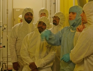
Subsequently, the group visited the IC and MEMS fabrication facilities under the guidance of Dr. Dariusz Szmigiel. This was a comprehensive 4-hour tour of IC/MEMS production facilities, including photolithography, ion implantation, etching, dicing and packaging equipment. On the right: ESRs in the photolithography lab. Left-to-right: B. Hussain, B. Milinkovic, A. Chandran, L. Manjakkal, D. Szmigiel (ITE, blue coat), A. Pajkanovic. |
 |
Second day summary
Following an explicit request from a group of ESRs, a course in design of semi-custom ASIC circuits has been organized. The course has been conducted by Dr. Phil Poole, Director of Semiconductors of MICRODUL AG (Switzerland).
 |
General agenda of the course:
|
Third day summary - part 1
The first part of the next day has been dedicated to continuation of the IC design seminar.
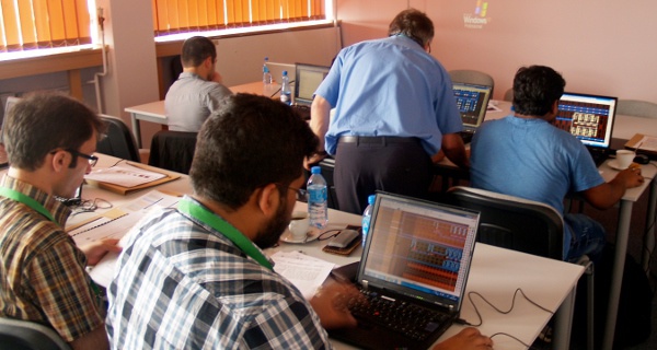 Above: MICRODUL seminar, left-to-right: I. Kianpour (INECS), A. Pajkanovic (UNS), B. Hussain (INESC), P. Poole (MICRODUL), A. Chandran (UNS).


